Custom PCB Design & Rapid Hardware Prototyping Services
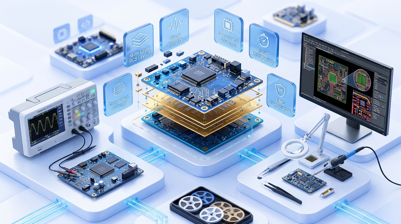
Flawless hardware starts with disciplined printed circuit board (PCB) layout. Exelon Circuits designs multi-layer, high-density PCBs engineered for signal integrity, thermal dissipation, and industrial electromagnetic compatibility (EMC).
From rapid in-house SMD prototyping and component sourcing to mass production manufacturing handoffs, our electronics engineering team in Surathkal brings your physical hardware visions to life.
PCB engineering & hardware capabilities
Comprehensive technical solutions engineered for security, reliability and measurable business outcomes.
Schematic Capture & Component Sourcing
Selecting globally accessible, production-viable components and structuring clear, modular electrical schematics.
Multi-Layer High-Density PCB Layout
Designing compact 2, 4, 6, and 8-layer boards with dedicated ground planes and optimized power distribution.
High-Speed Digital & RF Impedance Matching
Length tuning differential pairs (USB, Ethernet, PCIe) and calculating controlled microstrip RF impedance.
Thermal Management & Heat Dissipation
Integrating thermal vias, copper pours, and heat sink pads to ensure power semiconductors run cool and reliable.
EMC/EMI Pre-Compliance Design
Mitigating radiated emissions and noise interference to pass mandatory CE, FCC, and BIS compliance tests.
Design for Manufacturing (DFM) Checks
Verifying trace clearances, annular rings, drill sizes, and solder mask bridges against PCB fab house capabilities.
Rapid SMD Prototyping & Assembly
In-house stencil printing, reflow soldering, and microscope inspection for quick-turn prototype evaluation.
Production Gerber & BoM Handoff
Delivering verified Gerber files, IPC-2581 outputs, drill maps, pick-and-place XY data, and manufacturer BoMs.
Who needs custom PCB engineering
Enterprises and innovators building specialized physical electronics:
Hardware Product Startups
Transforming breadboard prototypes into compact, production-ready commercial circuit boards
Industrial Equipment Manufacturers
Replacing outdated relay panels with ruggedized, solid-state custom controller boards
IoT Sensor & Gateway Developers
Designing battery-efficient, miniature wireless sensor PCBs with integrated antennas
Our hardware engineering process
A disciplined, transparent delivery sequence ensuring predictable timelines and verified deliverables.
Specification & Component Selection
Defining electrical parameters, power sources, physical enclosure dimensions, and cost targets.
Schematic Design & Simulation
Drafting complete circuit schematics and running SPICE power simulations.
PCB Layout & Impedance Routing
Placing components, routing differential pairs, and optimizing thermal ground planes.
DFM Review & Fabrication
Submitting verified Gerbers to high-precision fabrication partners.
Assembly & Hardware Testing
Populating SMD components, verifying voltage rails, and flashing bring-up firmware in our Surathkal lab.
Proven Deployments & Results
Real client solutions engineered, tested, and running in production.
What Custom PCB Design Costs
PCB design projects are quoted based on layer count and routing complexity:
Why Partner with Exelon Circuits?
Local presence, certified engineering personnel, and dedicated post-deployment support.
Physical electronics engineering laboratory in Surathkal: hands-on assembly, rework, and microscope inspection
Complete design file ownership: you receive all Altium / KiCAD source files, schematics, and manufacturing outputs
Tight integration with our firmware developers: we design boards with debugging headers and test points for smooth bring-up
Local accessibility: discuss schematics and inspect physical prototype boards directly with our engineers in Mangalore
Frequently Asked Questions
Clear answers regarding deployment timelines, technical scope, and ongoing support.
Turn your hardware circuit concept into production reality
Schedule a schematic and hardware feasibility review with our PCB engineers.
Related Technical Reading
Engineering deep-dives, regulatory updates, and technical best practices.